

Reviewed by: Mechanical Engineering Team, Engon Technologies
Why IoT Enclosure Design Mistakes Increase Manufacturing Cost
You have a brilliant IoT product idea. You have funding, a team, and a rough prototype. But before you ever send a single unit to a customer, your budget is already bleeding out from the inside. The culprit? Your enclosure design—often developed without proper injection molding design input or the support of experienced injection molding design services —can lead to costly mistakes that only appear after manufacturing begins.
For hardware startups, the enclosure is rarely the first priority. Engineers focus on firmware, connectivity, and sensors. Designers obsess over the app interface. And the enclosure, the physical shell that holds everything together, gets treated as an afterthought.
That is a mistake that can become expensive. We’ve seen many product development teams encounter the same challenges: enclosure designs that perform well in CAD but create unexpected manufacturing, assembly, or reliability issues during production.
Our mechanical product engineering support for hardware startups helps identify these risks early through practical engineering expertise, enclosure validation, and design for manufacturability (DFM). Having worked with startups across the US and Europe, we’ve seen how resolving these issues before prototyping or tooling can significantly reduce redesign costs and accelerate product development. Here are seven common IoT enclosure design mistakes and practical ways to avoid them.
IoT enclosure design involves much more than creating a protective housing for electronics. Decisions related to operating environment, material selection, electronics integration, manufacturability, and tooling all influence production cost, product reliability, and time-to-market. Understanding these engineering considerations early helps reduce redesigns, improve manufacturing readiness, and support a smoother transition from prototype to production.
1. IoT Enclosure Design Mistake: No Clear Use-Case Definition
IP Rating & Waterproof Design Basics
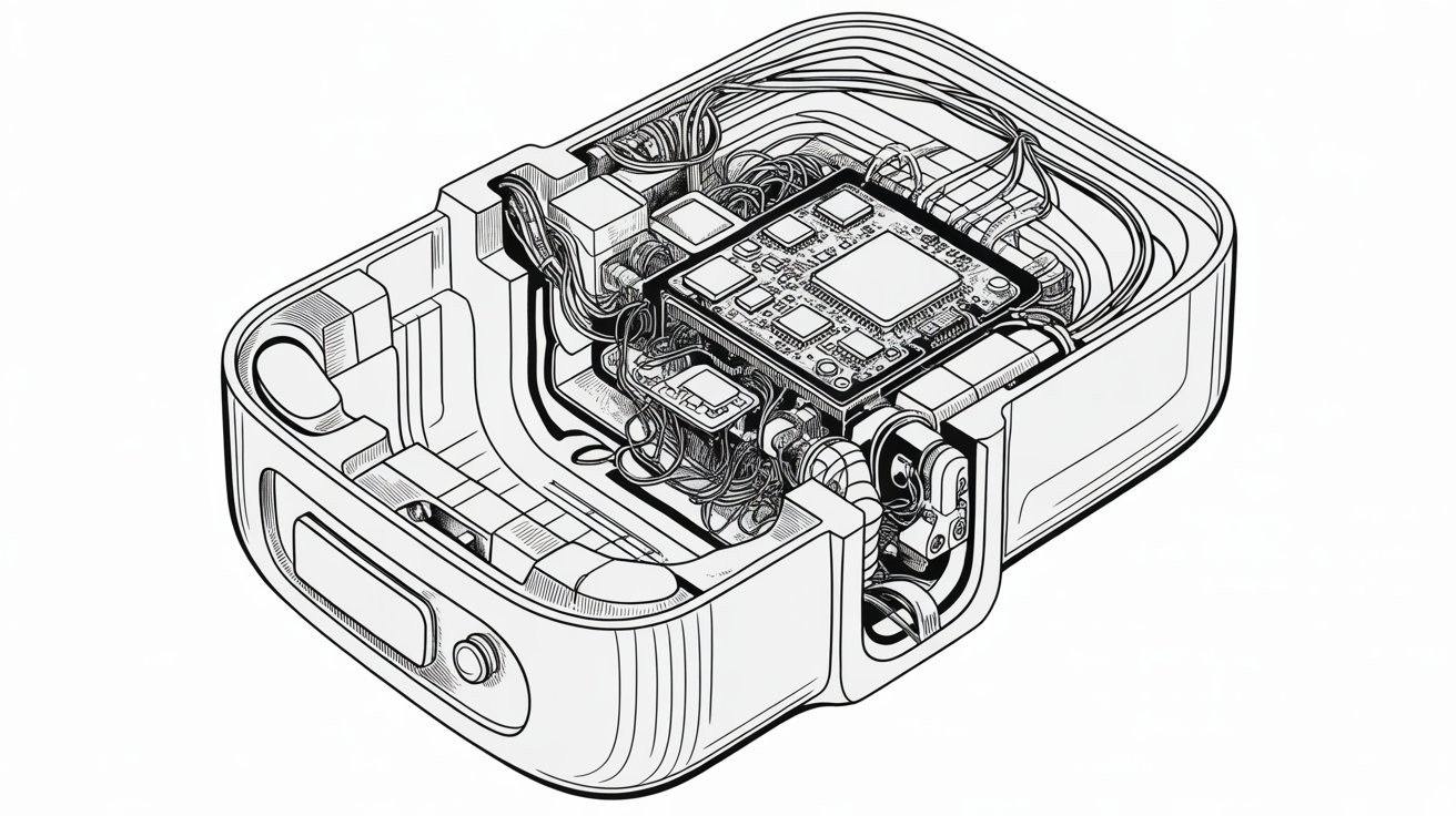
Every IoT enclosure design decision —from material selection and sealing methods to mounting features and structural geometry—starts with one fundamental question:
Where and how will this product actually be used?
Consider whether your device will be mounted on an indoor wall, installed on factory equipment, deployed on outdoor infrastructure, or used in agricultural environments exposed to rain, dust, sunlight, and temperature fluctuations. Each application creates different mechanical and environmental challenges, requiring an enclosure designed specifically for those operating conditions.
IP ratings are a good example. IP54, IP67, and IP68 are not interchangeable. Selecting a higher rating than necessary can increase manufacturing complexity and cost, while choosing insufficient protection may result in moisture ingress, premature product failure, and expensive field replacements.
One common observation during enclosure design reviews is that environmental requirements are often finalised after the enclosure concept has already been developed. When operating conditions change late in the project, engineering teams frequently need to revisit material selection, sealing methods, or enclosure geometry before production can begin. Addressing these requirements early helps reduce engineering changes, tooling modifications, and project delays.
Engineering Takeaway
Clearly defining the product’s operating environment before enclosure development begins provides a strong foundation for every design decision that follows. Material selection, environmental protection, structural design, and manufacturing methods are all influenced by how and where the product will be used. Establishing these requirements early reduces uncertainty and improves manufacturing readiness.
Note: The following engineering scenarios are illustrative examples based on common IoT enclosure design challenges observed across hardware product development. They are intended to demonstrate how early design decisions can affect manufacturability, reliability, and production readiness.
2. Poor Electronics–Enclosure Integration
Electronics Enclosure Design & Antenna Placement
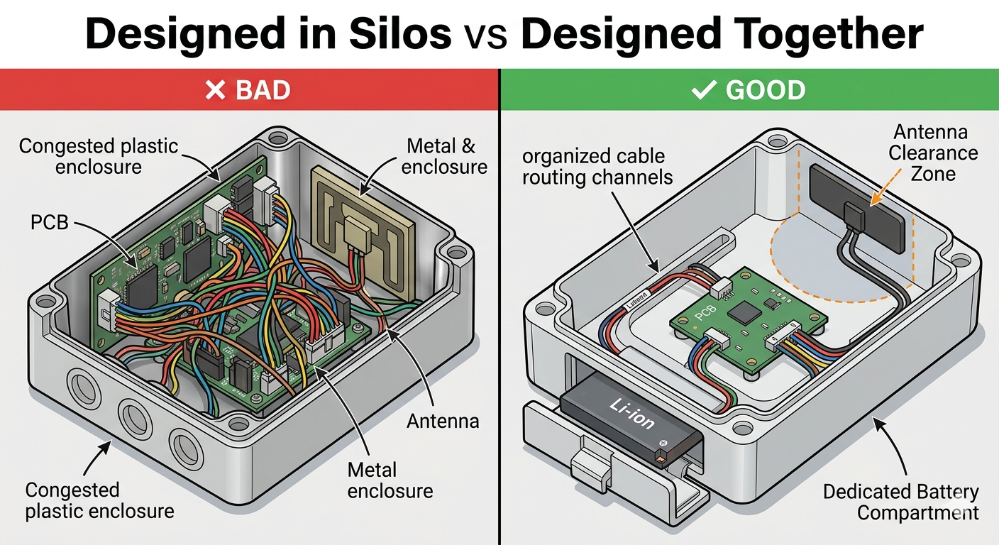
The PCB team designs the electronics, while the mechanical team develops the enclosure. When these activities happen independently with minimal collaboration, integration issues often appear during prototyping or production preparation. A well-coordinated PCB enclosure design process helps identify these conflicts before they become costly engineering changes.
Common problems include antennas positioned too close to enclosure walls, batteries with limited service access, cable routing that complicates assembly, or PCB mounting points that interfere with structural features. Although these issues may appear minor during CAD development, they can significantly affect product performance, manufacturability, and assembly efficiency.
Antenna placement deserves particular attention. Reliable antenna design for IoT requires adequate clearance and careful consideration of enclosure materials and internal component placement. Wireless technologies such as Wi-Fi, Bluetooth, LoRa, and LTE are highly sensitive to nearby materials and enclosure geometry, making early design decisions critical to consistent signal performance.
The most effective approach is to develop the enclosure and electronics as one integrated system rather than two independent projects. Working from a shared 3D model enables mechanical, electronics, and manufacturing teams to identify packaging conflicts, assembly challenges, and serviceability concerns before tooling begins.
Engineering Takeaway
An IoT enclosure should be designed alongside the electronics it protects. Early collaboration between engineering disciplines reduces redesign risk, improves manufacturability, and helps deliver a product that performs reliably in production.
3. Ignoring Manufacturing Numbers (Volume → Process → Design)
How to Reduce Manufacturing Cost in IoT Products
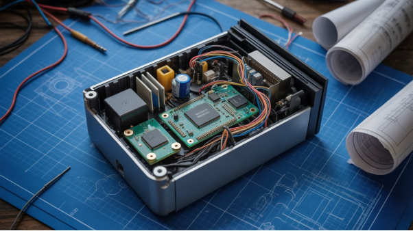
One of the earliest manufacturing decisions in hardware development is determining the expected production volume, because it influences every design decision that follows. Production volume determines the manufacturing process, and the chosen process defines the design constraints—this is the foundation of design for manufacturability (DFM). Designing for 100 units is fundamentally different from designing for 100,000.
For low-volume production, CNC machining and 3D printing are ideal. They require little or no tooling, support rapid design iterations, and help validate functionality before committing to production. The trade-off is a higher cost per part.
As production volumes increase, injection moulding becomes the more economical option because tooling costs are distributed across thousands of parts. However, this also introduces strict design requirements such as uniform wall thickness, draft angles, ribs, and simplified geometry, all of which directly influence injection molding cost.
One of the most common manufacturing mistakes is approving prototype parts without considering how they will be produced at scale. Features that are easy to machine or 3D print may require significant redesign before injection moulding, leading to tooling modifications, production delays, and additional cost. Engaging injection molding design services early helps identify these issues before tooling begins, reducing manufacturing risk and improving production readiness.
Engineering Takeaway
Production volume should guide manufacturing decisions from the beginning. Following the sequence Volume → Process → Design helps control tooling costs, minimise redesigns, and create products that scale efficiently.
4. Material Selection Mistake: Choosing the Wrong Material Early
ABS vs Polycarbonate for Enclosures
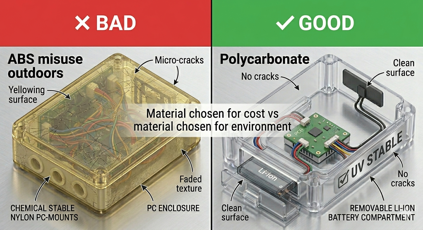
Many enclosure failures can be traced back to material decisions made during the early design stage. Selecting a plastic based primarily on cost or familiarity, rather than the product’s operating environment, often leads to reliability issues that become expensive to correct after tooling is complete. This makes plastic material selection one of the most important decisions in hardware design.
ABS is one of the most widely used thermoplastics for consumer electronics enclosures. It is affordable, easy to mould, and provides a good cosmetic finish. However, it has limitations, including poor UV resistance, lower impact strength, and limited chemical resistance. These trade-offs often become apparent when products are deployed outdoors or in demanding industrial environments.
Polycarbonate offers significantly better impact resistance and UV stability, making it a better choice for outdoor and industrial applications. Nylon (PA66) performs well where components are exposed to mechanical stress or chemicals. Each material also affects tooling requirements, processing conditions, and overall manufacturing cost.
During enclosure validation, engineers often find that a material selected for a successful prototype does not meet the long-term durability requirements of the final product. Involving injection molding design services early helps align material properties with functional, environmental, and manufacturing requirements before tooling investment begins.
Engineering Takeaway
Material selection should be driven by the product’s operating environment, not simply by material cost or familiarity. Choosing the right plastic early improves product reliability, reduces manufacturing risk, and helps avoid expensive redesigns later in development.
5. Product Design Mistake: Over-Engineering at MVP Stage
How to Reduce Manufacturing Cost in IoT Products
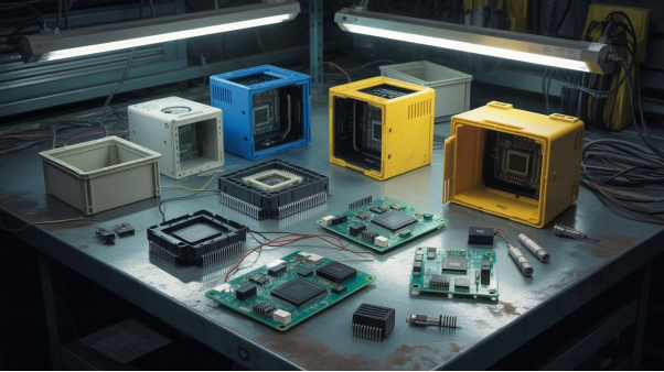
Hardware founders are often perfectionists. While that mindset is valuable when preparing for production, it can become an expensive mistake during hardware MVP development.
The purpose of an MVP is to validate the product’s core assumptions. Does it solve the intended problem? Does the technology perform reliably in real-world conditions? Will customers use it? At this stage, the enclosure only needs to answer those questions—not showcase production-level aesthetics.
A common mistake is investing in premium enclosure features too early. Multi-part assemblies, cosmetic finishes, embossed logos, and complex snap-fit mechanisms increase prototyping costs without providing additional validation. During prototype development, many of these features are later simplified or removed because they increase complexity without improving product validation.
For most MVPs, a simple two-part 3D-printed or vacuum-cast enclosure produced using rapid prototyping methods is sufficient to protect the electronics and demonstrate functionality. As the product matures and customer feedback is validated, the enclosure can be refined for manufacturability, aesthetics, and volume production.
Early engineering guidance through mechanical product engineering services for startups in the US & Europe helps ensure design decisions remain practical, manufacturable, and scalable, reducing the risk of costly redesigns before production.
Engineering Takeaway
An MVP should validate the product, not perfect it. Keeping the enclosure simple reduces development costs, shortens iteration cycles, and provides the flexibility to refine the design with confidence before investing in production tooling.
6. Industrial Design Mistake: Underestimating Its Impact
Ergonomics & Product Perception
Many technically sound products require redesign not because the electronics fail, but because users find them uncomfortable, unintuitive, or difficult to use. This is why industrial design services are an essential part of successful product development.
Industrial design extends beyond appearance. It combines ergonomics, usability, and form to create products that feel natural in everyday use. A product may perform reliably, but if buttons are difficult to reach, the grip feels awkward, or the interface is confusing, users quickly lose confidence.
During prototype evaluations, factors such as grip profile, button placement, display visibility, and weight distribution are evaluated alongside engineering and manufacturing requirements. These decisions influence usability, perceived quality, and overall product acceptance.
Effective product design services balance user expectations with engineering feasibility and manufacturability, resulting in products that are intuitive to use, practical to manufacture, and aligned with market needs.
Engineering Takeaway
Successful products combine engineering performance with a positive user experience. Addressing industrial design early improves usability, strengthens product perception, and reduces costly design changes before production.
7. Investing in Production Tooling Too Early
When to Use Injection Molding vs 3D Printing
One of the most expensive enclosure decisions is committing to production tooling before the design has been fully validated. Injection moulding is the right manufacturing process for high-volume production, but it is rarely the right choice during the early stages of product development.
Prototype vs Production Manufacturing
| Prototype Validation | Production Manufacturing |
|---|---|
| 3D Printing (FDM, SLA, SLS) | Injection Moulding |
| Minimal tooling investment | High tooling investment |
| Fast design iterations | Design changes are expensive |
| Ideal for functional testing | Ideal for high-volume production |
| Suitable for MVPs and pilot builds | Suitable for validated production designs |
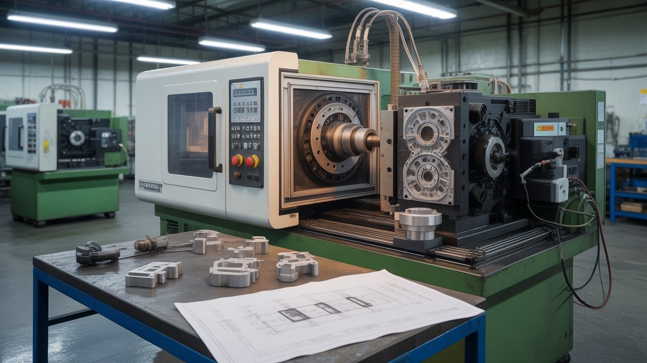
A production mould for a typical IoT enclosure can cost $15,000 to $50,000 or more. Once the tool is cut, even relatively small design changes can require costly modifications, while major revisions may require an entirely new mould. Validating the enclosure and engaging injection molding design services before tooling begins helps reduce development risk and avoid unnecessary tooling costs.
A structured design review before releasing tooling can uncover manufacturability, assembly, and tolerance issues while design changes are still inexpensive. Read our guide on design review mistakes that lead to costly production delays to learn how engineering teams avoid these common pitfalls.
During prototype testing, improvements related to enclosure fit, assembly, component access, and manufacturability are often identified. Making these changes after steel tooling has been commissioned is both expensive and time-consuming. Using rapid prototyping services with FDM, SLA, or SLS printing allows teams to refine the enclosure quickly before committing to production, while vacuum casting provides small batches in production-like materials for pilot testing and customer evaluation.
Engineering Takeaway
Validate the enclosure thoroughly before investing in production tooling. A prototype-first approach reduces tooling costs, shortens development cycles, and minimises expensive design changes during production.
Key Takeaways
- Define the product’s operating environment before designing the enclosure.
- Develop the PCB and enclosure as one integrated system from the beginning.
- Choose enclosure materials based on operating conditions, not just cost or familiarity.
- Align the enclosure design with the intended manufacturing process and production volume.
- Validate prototypes thoroughly before investing in production tooling.
- Consider ergonomics, usability, and manufacturability throughout the design process.
If you are developing an IoT product and need support with enclosure design, mechanical integration, DFM, or production readiness, our Mechanical Product Engineering Services help hardware teams identify risks early and move from prototype to manufacturing with greater confidence.
The Common Thread
Although each mistake is different, they all stem from the same issue: treating the enclosure as an afterthought instead of an integral part of the product. Successful IoT enclosure design begins with a clear understanding of the product’s use case, operating environment, manufacturing strategy, and long-term reliability.
Planning for electronics integration, material selection, thermal management, manufacturability, and regulatory requirements from the outset helps reduce redesigns and production delays. Validating prototypes before investing in tooling also gives teams the flexibility to refine the design when changes are still quick and cost-effective.
Having supported hardware startups across the US and Europe, we’ve seen how structured enclosure development process helps identify enclosure design risks long before production begins.
At Engon Technologies we help startups turn product concepts into manufacturable, scalable designs by addressing these challenges early in the development process.