
Why IoT Enclosure Design Mistakes Increase Injection Molding Cost
You have a brilliant IoT product idea. You have funding, a team, and a rough prototype. But before you ever send a single unit to a customer, your budget is already bleeding out from the inside. The culprit? Your enclosure design—often developed without proper injection molding design input or the support of experienced injection molding design services —can lead to costly mistakes that only appear after manufacturing begins.
For hardware startups, the enclosure is rarely the first priority. Engineers focus on firmware, connectivity, and sensors. Designers obsess over the app interface. And the enclosure, the physical shell that holds everything together, gets treated as an afterthought.
That is a mistake that costs real money. We have worked with startups across the US and Europe, and we have seen the same painful patterns repeat. —especially for teams looking for mechanical product engineering support for hardware startups Here are the seven most expensive IoT enclosure design mistakes and how to avoid every single one.
1. IoT Enclosure Design Mistake: No Clear Use-Case Definition
IP Rating & Waterproof Design Basics
Every design decision your IoT enclosure design demands, the material, the sealing, and the mounting points flow directly from one foundational question: Where and how will this device actually live in the real world?
Too many startups skip this step. They design in a lab, test in a controlled environment, and assume the field will be forgiving. It never is.
Consider whether your device will be mounted on a wall indoors or bolted to a utility pole in the rain. Will it sit on a factory floor with constant vibration or in a hospital room that gets wiped with harsh chemicals? Will users handle it daily, or will it sit untouched for three years? Each scenario demands a completely different enclosure strategy, and getting it wrong means starting over.
IP ratings are a good example of this. IP54, IP67, and IP68 are not interchangeable. IP54 handles splashing water; IP67 means submersion up to one meter for thirty minutes. Choosing the wrong rating and you will result in either overspending on unnecessary protection or watching your field devices fail in the first rainy season when a proper waterproof enclosure would have prevented failure.
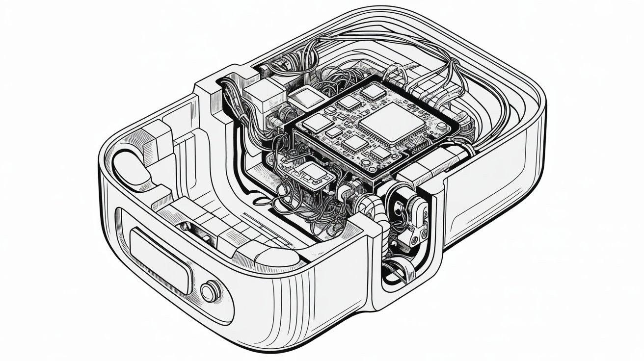
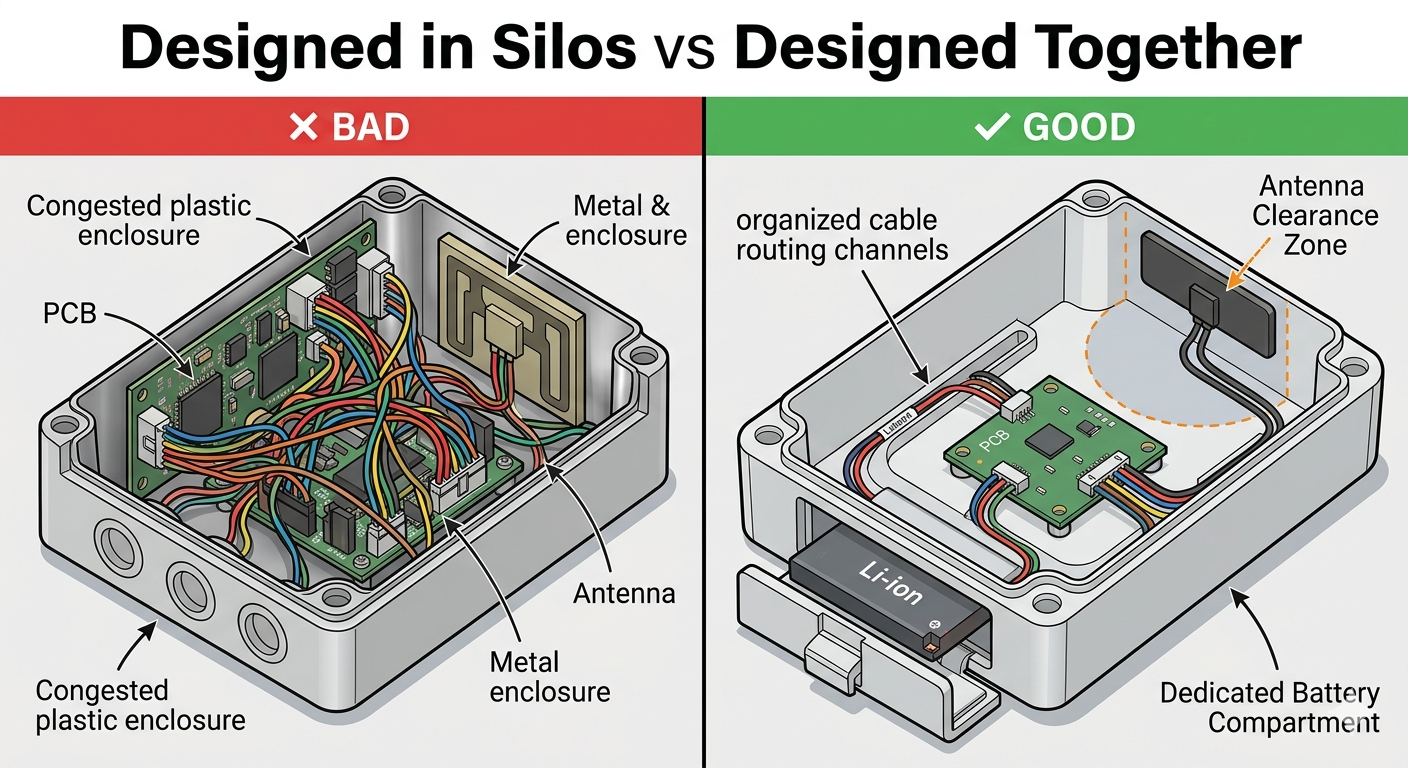
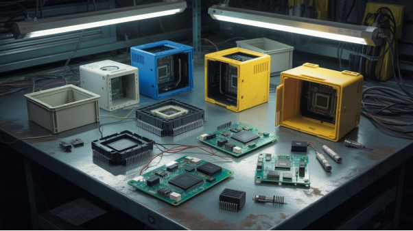
2. Injection Molding Design Mistake: Poor Electronics–Enclosure Integration
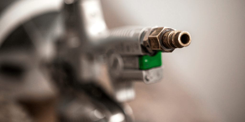
Electronics Enclosure Design & Antenna Placement
The PCB team designs the PCB. The mechanical team designs the enclosure. They share files the week before prototype submission. The result is antennas pressed against metal walls, batteries wedged in with no access panel, and cable routes that require impossible bends common issues in poor PCB enclosure design.
Antenna placement deserves particular attention. IoT devices depend on Wi-Fi, BLE, LoRa, and LTE, and signal performance is devastatingly sensitive to nearby materials. A polycarbonate wall has minimal impact. A metal enclosure without carefully positioned antenna clearance can cut signal strength by 40% or more, exactly as the Berlin case below demonstrates highlighting the importance of proper antenna design for IoT.
The fix is co-design from day one. Mechanical, electronics, and tool design teams must work on a shared 3D model and align on internal layout constraints before finalising their designs to avoid conflicts and rework.
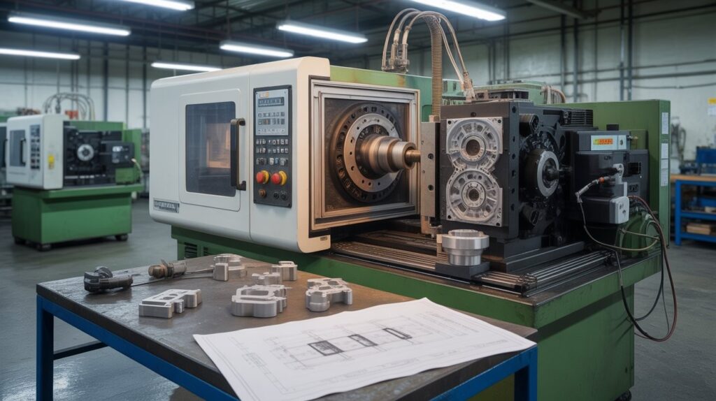
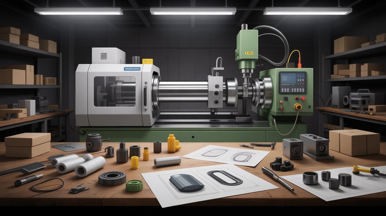
Injection Molding Cost Mistake: Ignoring Manufacturing Numbers
Everything in hardware development is driven by numbers. Production volume determines the manufacturing process, and the chosen process directly defines your design constraints —this is the core of design for manufacturing (DFM). Designing for 100 units is completely different from designing for 100,000 units.
At low volumes, flexible methods like CNC machining or 3D printing are ideal. They require little to no tooling, allow rapid design changes, and help validate functionality and market fit. However, the per-unit cost remains high.
At high volumes, processes like injection moulding become viable. While they significantly reduce per-unit cost, they require high upfront tooling investment and strict adherence to design rules such as uniform wall thickness, draft angles, and simplified geometry —factors that directly impact overall injection molding cost.
Ignoring this relationship leads to costly mistakes—designs optimized for the wrong process, expensive tooling rework, and production delays,and avoidable manufacturing defects. Startups that involve injection molding design services early can identify these issues before tooling begins, saving significant time and cost during production scaling.
In short: Volume → Process → Design.
Getting this sequence right is critical to controlling cost and scaling successfully
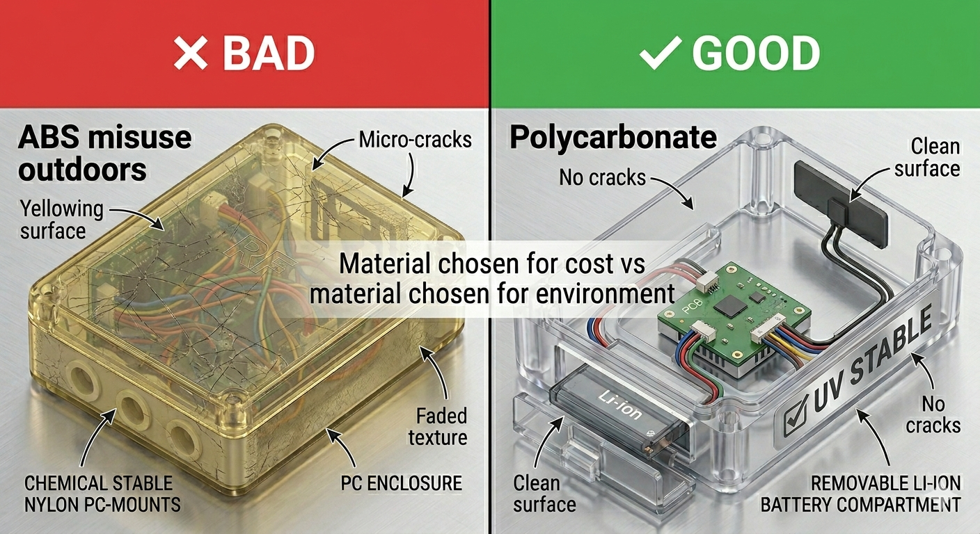
4. Material Selection Mistake: Choosing the Wrong Material Early
ABS vs Polycarbonate for Enclosures
Not all plastics are created equal, and the difference between a good material choice and a poor one can mean the difference between a product that lasts five years in the field and one that cracks after six months —making plastic material selection a critical decision in hardware design.
ABS is the most commonly used thermoplastic in consumer electronics enclosures. It is affordable, easy to mould, and takes paint well. But it has real weaknesses: poor UV resistance (it yellows and becomes brittle under sunlight), limited chemical resistance, and lower impact strength compared to alternatives. These trade-offs are often overlooked without proper injection molding design services guiding early material decisions.
Polycarbonate offers dramatically better impact resistance and UV stability, making it the right choice for outdoor and industrial deployments. Nylon (PA66) excels in environments with mechanical stress and chemical exposure. Each material carries different cost implications, both for the raw material itself and for tooling and processing.
The critical mistake startups make is choosing a material based on cost or familiarity, without mapping it against actual environmental requirements. Material selection must be tied to the use-case definition. Get that wrong, and you face expensive retooling and delayed timelines.
5. Product Design Mistake: Over-Engineering at MVP Stage
How to Reduce Manufacturing Cost in IoT Products
Hardware founders are often perfectionists. That quality is an asset at scale, but at the MVP stage, it is a budget killer especially in hardware MVP development.
The purpose of a hardware MVP is to validate your core assumptions. Does the device solve the problem? Do customers want it? Does the technology work reliably enough in real conditions? Your enclosure at this stage needs to answer those questions, nothing more.
When startups design premium enclosures for their MVP complex multi-part assemblies, high-gloss finishes, embossed logos, and elaborate snap-fit mechanisms, they multiply their prototyping costs by two or three times without gaining any validation data. Worse, they lock themselves into design decisions that may need to be reversed once actual customer feedback arrives.
No two hardware products are the same—and treating them that way leads to costly mistakes.
Every product has unique requirements: environment, usage, regulations, scale, and cost. That’s why a one-size-fits-all approach fails. The right approach is to plan upfront—understand how the product will be used, what conditions it will face, and how it will be manufactured.
Expert input at this stage is critical. The right support—delivered through mechanical product engineering services for startups in the US & Europe—ensures your design decisions are practical, scalable, and aligned with real market requirements from day one. It also helps uncover hidden risks such as tooling constraints, assembly challenges, and compliance gaps early, preventing costly redesigns later.
Rushing into design leads to rework and delays. In hardware, what you decide upfront defines everything that follows.
A two-part 3D-printed or vacuum-cast enclosure that houses your electronics securely is perfectly adequate for proving your concept using rapid prototyping methods. Save the premium industrial design investment for when you have confirmed product-market fit and are ready for volume production.
6. Industrial Design Mistake: Underestimating Its Impact
Ergonomics & Product Perception
Products don’t just need to function—they need to create the right perception. Users often judge quality within seconds based on how a product looks and feels, making industrial design services a critical factor in success.
Industrial design goes beyond aesthetics. It integrates form, ergonomics, usability, and interaction to create a seamless user experience. A product that looks premium but feels uncomfortable or confusing will fail just as quickly as one that works well but appears cheap or outdated.
Good design aligns the product with user expectations. It considers how the product is held, used, and perceived in real-world contexts. This balance between visual appeal and functionality builds trust, improves usability, and drives adoption something effective product design services are built to achieve.
Ignoring industrial design leads to poor first impressions, lower perceived value, and reduced market acceptance.
In short: Perception + Function + User = Successful Design.
7. Injection Molding Mistake: Tooling Too Early
When to Use Injection Molding vs 3D Printing
Injection moulding is the right process for high-volume production. It is seldom the right choice for early-stage validation. A production mould tool for a typical IoT enclosure costs $15,000 to $50,000 or more. Once cut in steel, design changes are expensive, and some require a completely new tool. Startups that commit to tooling too early —often without proper injection molding design services or validation— become reluctant to make necessary changes and lock their mistakes in metal.
The smarter path: validate aggressively before committing. FDM, SLA, or SLS printing enables rapid iteration at minimal cost using rapid prototyping services. Vacuum casting produces small batches of ten to fifty units in production-grade materials, ideal for real-world pilot programs. Only invest in production tooling when the design is thoroughly validated mechanically, thermally, and in genuine user conditions.

The Common Thread
Every mistake here shares the same root: treating the enclosure as an afterthought instead of a core system. Define your use case before you design. Integrate electronics and enclosure from day one. Plan for thermal management, material performance, and compliance requirements early. Validate before committing to production tooling. Keep your MVP simple enough to actually prove what needs proving.
A structured enclosure design process guided by engineers who understand the full lifecycle from concept to certification such as Engon Technologies can save startups $20,000 to $200,000 in avoidable mistakes before manufacturing even begins.